SOI is the abbreviation for Silicon-On-Insulator. Literally, it means “silicon on an insulator.” In practice, the structure is that there is an ultra-thin insulating layer, such as SiO₂, on top of the silicon wafer, and then a thin silicon layer is formed on top of this insulating layer. This structure separates the active silicon layer from the silicon substrate. In a traditional silicon process, however, the chip is formed directly on the silicon substrate without using an insulating layer.
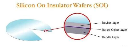
SOI wafer is composed of three key structural layers: a single-crystal silicon device layer, a silicon dioxide insulating layer (the buried oxide, or BOX), and a silicon substrate. Together, these three layers form an independent and stable electrical environment, with each layer playing its own role while working in synergy to enhance overall performance and reliability.
The top single-crystal silicon device layer (typically about 5 nm to 2 μm thick) is the core region where transistors and other active devices are fabricated. Its ultra-thin structure is a crucial foundation for improving device performance and enabling continuous scaling.
The middle buried oxide (BOX) layer provides electrical isolation. This silicon dioxide layer, usually 5 nm to 2 μm in thickness, effectively blocks electrical coupling between the device layer and the underlying substrate through both physical and chemical isolation mechanisms.
The bottom silicon substrate mainly provides structural rigidity and mechanical stability, ensuring wafer reliability during manufacturing and subsequent operation. Its thickness is generally in the range of 200 μm to 700 μm, offering sufficient mechanical support while taking processability and application requirements into account.
Main Advantages of SOI Wafers
1. Higher Speed
- With a buried oxide layer beneath the devices, the transistors are isolated from the silicon substrate. This reduces parasitic capacitance, speeds up switching, and makes SOI well-suited for high-speed logic and RF circuits.
2. Lower Power Consumption
- Smaller capacitance means lower charging and discharging losses.
- Fewer leakage paths lead to reduced standby (static) power consumption, making the system more power-efficient.
3. Better Isolation
- Each device is “sitting” on an oxide layer, which greatly reduces electrical interference between devices. This improves stability when integrating analog + digital circuits, power management units, and RF modules on the same chip.
4. Improved Radiation and High-Temperature Tolerance
- Radiation-generated charges are less likely to spread through the substrate, making SOI devices safer and more reliable in high-radiation environments such as aerospace.
- The increase in leakage current at high temperatures is less severe, which is beneficial for automotive electronics and industrial control applications.
5. Favorable for Further Scaling
- With a very thin silicon layer on top and a buried oxide layer beneath, short-channel effects are better controlled, making it easier to maintain stable device behavior as process nodes continue to shrink.
SOI technology has already been applied across multiple fields. In consumer electronics, it is used in the RF front-end modules of smartphones, such as 5G filters. In automotive electronics, it provides a stable process platform for in-vehicle radar chips. In the aerospace sector, it is employed in high-reliability satellite communication equipment. In medical devices, SOI supports the design and implementation of implantable medical sensors and various types of low-power monitoring chips.
Our company offers custom projects for single-crystal silicon carrier wafers:
-
Silicon substrate thickness: 100 μm / 300 μm / 400 μm / 500 μm / 625 μm and above
-
SiO₂ thickness: from 100 nm to 10 μm
-
Active silicon layer: ≥ 20 nm
Media Contact
Company Name: Ningbo VET Energy Technology Co., Ltd
Email:Send Email
Country: China
Website: https://www.vet-china.com/